VTR Quick Start
This is a quick introduction to VTR which covers how to run VTR and some if its associated tools (VPR, Odin II, ABC).
Setting Up VTR
Download VTR
The first step is to download VTR and extract VTR on your local machine.
Note
Developers planning to modify VTR should clone the VTR git repository.
Build VTR
On most unix-like systems you can run:
> make
from the VTR root directory (hereafter referred to as $VTR_ROOT) to build VTR.
Note
In the VTR documentation lines starting with > (like > make above), indicate a command (i.e. make) to run from your terminal.
When the \ symbol appears at the end of a line, it indicates line continuation.
Note
$VTR_ROOT refers to the root directory of the VTR project source tree. To run the examples in this guide on your machine, either:
define VTR_ROOT as a variable in your shell (e.g. if
~/trees/vtris the path to the VTR source tree on your machine, run the equivalent ofVTR_ROOT=~/trees/vtrin BASH) which will allow you to run the commands as written in this guide, ormanually replace $VTR_ROOT in the example commandss below with your path to the VTR source tree.
Note
If VTR fails to build you may need to install the required dependencies.
For more details on building VTR on various operating systems/platforms see Building VTR.
Running VPR
Lets now try taking a simple pre-synthesized circuit (consisting of LUTs and Flip-Flops) and use the VPR tool to implement it on a specific FPGA architecture.
Running VPR on a Pre-Synthesized Circuit
First, lets make a directory in our home directory where we can work:
#Move to our home directory
> cd ~

#Make a working directory
> mkdir -p vtr_work/quickstart/vpr_tseng

#Move into the working directory
> cd ~/vtr_work/quickstart/vpr_tseng
Now, lets invoke the VPR tool to implement:
the
tsengcircuit ($VTR_ROOT/vtr_flow/benchmarks/blif/tseng.blif), onthe
EArchFPGA architecture ($VTR_ROOT/vtr_flow/arch/timing/EArch.xml).
We do this by passing these files to the VPR tool, and also specifying that we want to route the circuit on a version of EArch with a routing architecture channel width of 100 (--route_chan_wdith 100):
> $VTR_ROOT/vpr/vpr \
    $VTR_ROOT/vtr_flow/arch/timing/EArch.xml \
    $VTR_ROOT/vtr_flow/benchmarks/blif/tseng.blif \
    --route_chan_width 100
This will produce a large amount of output as VPR implements the circuit, but you should see something similar to:
VPR FPGA Placement and Routing.
Version: 8.1.0-dev+2b5807ecf
Revision: v8.0.0-1821-g2b5807ecf
Compiled: 2020-05-21T16:39:33
Compiler: GNU 7.3.0 on Linux-4.15.0-20-generic x86_64
Build Info: release VTR_ASSERT_LEVEL=2

University of Toronto
verilogtorouting.org
vtr-users@googlegroups.com
This is free open source code under MIT license.

#
#Lots of output trimmed for brevity....
#

Geometric mean non-virtual intra-domain period: 6.22409 ns (160.666 MHz)
Fanout-weighted geomean non-virtual intra-domain period: 6.22409 ns (160.666 MHz)

VPR suceeded
The entire flow of VPR took 3.37 seconds (max_rss 40.7 MiB)
which shows that VPR as successful (VPR suceeded), along with how long VPR took to run (~3 seconds in this case).
You will also see various result files generated by VPR which define the circuit implementation:
> ls *.net *.place *.route

tseng.net  tseng.place  tseng.route
along with a VPR log file which contains what VPR printed when last invoked:
> ls *.log

vpr_stdout.log
and various report files describing the characteristics of the implementation:
> ls *.rpt

packing_pin_util.rpt              report_timing.hold.rpt   report_unconstrained_timing.hold.rpt
pre_pack.report_timing.setup.rpt  report_timing.setup.rpt  report_unconstrained_timing.setup.rpt
Visualizaing Circuit Implementation
Note
This section requires that VPR was compiled with graphic support. See VPR Graphics for details.
The .net, .place and .route files (along with the input .blif and architecture .xml files) fully defined the circuit implementation.
We can visualize the circuit implementation by:
Re-running VPR’s analysis stage (
--analysis), andenabling VPR’s graphical user interface (
--dispon).
This is done by running the following:
> $VTR_ROOT/vpr/vpr \
    $VTR_ROOT/vtr_flow/arch/timing/EArch.xml \
    $VTR_ROOT/vtr_flow/benchmarks/blif/tseng.blif \
    --route_chan_width 100 \
    --analysis --disp on
which should open the VPR graphics and allow you to explore the circuit implementation.
As an exercise try the following:
View the connectivity of a block (connections which drive it, and those which it drives)
View the internals of a logic block (e.g. try to find the LUTs/
.namesand Flip-Flops/.latch)Visualize all the routed circuit connections
See also
For more details on the various graphics options, see VPR Graphics
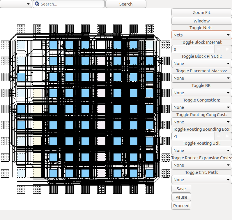
Fig. 1 Routed net connections of tseng on EArch.
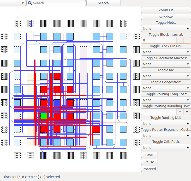
Fig. 2 Input (blue)/output (red) nets of block n_n3199 (highlighted green).
Note
If you do not provide --analysis, VPR will re-implement the circuit from scratch.
If you also specify --disp on, you can see how VPR modifies the implementation as it runs.
By default --disp on stops at key stages to allow you to view and explore the implementation.
You will need to press the Proceed button in the GUI to allow VPR to continue to the next stage.
Running the VTR Flow
In the previous section we have implemented a pre-synthesized circuit onto a pre-existing FPGA architecture using VPR, and visualized the result. We now turn to how we can implement our own circuit on a pre-existing FPGA architecture.
To do this we begin by describing a circuit behaviourly using the Verilog Hardware Description Language (HDL). This allows us to quickly and consisely define the circuit’s behaviour. We will then use the VTR Flow to synthesize the behavioural Verilog description it into a circuit netlist, and implement it onto an FPGA.
Example Circuit
We will use the following simple example circuit, which causes it’s output to toggle on and off:
1 2 3 4 5 6 7 8 9 10 11 12 13 14 15 16 17 18 19 20 21 22 23 24 25 26 27 28 29 30 | //A simple cricuit which blinks an LED on and off periodically
module blink(
input clk, //Input clock
input i_reset, //Input active-high reset
output o_led); //Output to LED
//Sequential logic
//
//A reset-able counter which increments each clock cycle
reg[4:0] r_counter;
always @(posedge clk) begin
if (i_reset) begin //When reset is high, clear counter
r_counter <= 5'd0;
end else begin //Otherwise increment counter each clock (note that it will overflow back to zero)
r_counter <= r_counter + 1'b1;
end
end
//Combinational logic
//
//Drives o_led high if count is below a threshold
always @(*) begin
if (r_counter < 5'd16) begin
o_led <= 1'b1;
end else begin
o_led <= 1'b0;
end
end
endmodule
|
This Verilog creates a sequential 5-bit register (r_counter) which increments every clock cycle.
If the count is below 16 it drives the output (o_led) high, otherwise it drives it low.
Manually Running the VTR Flow
Lets start by making a fresh directory for us to work in:
> mkdir -p ~/vtr_work/quickstart/blink_manual
> cd ~/vtr_work/quickstart/blink_manual
Next we need to run the three main sets of tools:
Odin II performs ‘synthesis’ which converts our behavioural Verilog (
.vfile) into a circuit netlist (.bliffile) consisting of logic equations and FPGA architecture primitives (Flip-Flops, adders etc.),ABC performs ‘logic optimization’ which simplifies the circuit logic, and ‘technology mapping’ which converts logic equations into the Look-Up-Tables (LUTs) available on an FPGA, and
VPR which performs packing, placement and routing of the circuit to implement it on the targetted FPGA architecture.
Synthesizing with ODIN II
First we’ll run ODIN II on our Verilog file to synthesize it into a circuit netlist, providing the options:
-a $VTR_ROOT/vtr_flow/arch/timing/EArch.xmlwhich specifies what FPGA architecture we are targetting,
-V $VTR_ROOT/doc/src/quickstart/blink.vwhich specifies the verilog file we want to synthesize, and
-o blink.odin.blifwhich specifies the name of the generated.blifcircuit netlist.
The resulting command is:
> $VTR_ROOT/ODIN_II/odin_II \
    -a $VTR_ROOT/vtr_flow/arch/timing/EArch.xml \
    -V $VTR_ROOT/doc/src/quickstart/blink.v \
    -o blink.odin.blif
which when run should end with something like:
Total time: 14.7ms
Odin ran with exit status: 0
Odin II took 0.01 seconds (max_rss 5.1 MiB)
where Odin ran with exit status: 0 indicates Odin successfully synthesized our verilog.
We can now take a look at the circuit which ODIN produced (blink.odin.blif).
The file is long and likely harder to follow than our code in blink.v; however it implements the same functionality.
Some interesting highlights are shown below:
blink.odin.blif (implements part of r_counter in blink.v)¶.latch blink^nMUX~0^MUX_2~23 blink^r_counter~0_FF re blink^clk 3
.latch blink^nMUX~0^MUX_2~27 blink^r_counter~4_FF re blink^clk 3
blink.odin.blif, used to perform addition (implements part of the + operator in blink.v)¶.subckt adder a[0]=blink^r_counter~0_FF b[0]=vcc cin[0]=blink^ADD~2-0[0]\
cout[0]=blink^ADD~2-1[0] sumout[0]=blink^ADD~2-1[1]
.subckt adder a[0]=blink^r_counter~1_FF b[0]=gnd cin[0]=blink^ADD~2-1[0]\
cout[0]=blink^ADD~2-2[0] sumout[0]=blink^ADD~2-2[1]
blink.odin.blif, implementing logical OR (implements part of the < operator in blink.v)¶.names blink^LT~4^GT~10 blink^LT~4^GT~12 blink^LT~4^GT~14 blink^LT~4^GT~16 blink^LT~4^GT~18 blink^LT~4^lOR~9
1---- 1
-1--- 1
--1-- 1
---1- 1
----1 1
See also
For more information on the BLIF file format see BLIF Netlist (.blif).
Optimizing and Technology Mapping with ABC
Next, we’ll optimize and technology map our circuit using ABC, providing the option:
-c <script>, where<script>is a set of commands telling ABC how to synthesize our circuit.
We’ll use the following, simple ABC commands:
read blink.odin.blif;                               #Read the circuit synthesized by ODIN
if -K 6;                                            #Technology map to 6 input LUTs (6-LUTs)
write_hie blink.odin.blif blink.abc_no_clock.blif   #Write new circuit to blink.abc_no_clock.blif
Note
Usually you should use a more complicated script (such as that used by run_vtr_flow) to ensure ABC optitmizes your circuit well.
The corresponding command to run is:
> $VTR_ROOT/abc/abc \
    -c 'read blink.odin.blif; if -K 6; write_hie blink.odin.blif blink.abc_no_clock.blif'
When run, ABC’s output should look similar to:
ABC command line: "read blink.odin.blif; if -K 6; write_hie blink.odin.blif blink.abc_no_clock.blif".

Hierarchy reader converted 6 instances of blackboxes.
The network was strashed and balanced before FPGA mapping.
Hierarchy writer reintroduced 6 instances of blackboxes.
If we now inspect the produced BLIF file (blink.abc_no_clock.blif) we see that ABC was able to significantly simplify and optimize the circuit’s logic (compared to blink.odin.blif):
1 2 3 4 5 6 7 8 9 10 11 12 13 14 15 16 17 18 19 20 21 22 23 24 25 26 27 28 29 30 31 32 33 34 35 36 37 38 39 40 41 42 43 44 45 46 | # Benchmark "blink" written by ABC on Tue May 19 15:42:50 2020
.model blink
.inputs blink^clk blink^i_reset
.outputs blink^o_led
.latch n19 blink^r_counter~0_FF 2
.latch n24 blink^r_counter~4_FF 2
.latch n29 blink^r_counter~3_FF 2
.latch n34 blink^r_counter~2_FF 2
.latch n39 blink^r_counter~1_FF 2
.subckt adder a[0]=blink^r_counter~0_FF b[0]=vcc cin[0]=blink^ADD~2-0[0] cout[0]=blink^ADD~2-1[0] sumout[0]=blink^ADD~2-1[1]
.subckt adder a[0]=blink^r_counter~1_FF b[0]=gnd cin[0]=blink^ADD~2-1[0] cout[0]=blink^ADD~2-2[0] sumout[0]=blink^ADD~2-2[1]
.subckt adder a[0]=blink^r_counter~2_FF b[0]=gnd cin[0]=blink^ADD~2-2[0] cout[0]=blink^ADD~2-3[0] sumout[0]=blink^ADD~2-3[1]
.subckt adder a[0]=blink^r_counter~3_FF b[0]=gnd cin[0]=blink^ADD~2-3[0] cout[0]=blink^ADD~2-4[0] sumout[0]=blink^ADD~2-4[1]
.subckt adder a[0]=blink^r_counter~4_FF b[0]=gnd cin[0]=blink^ADD~2-4[0] cout[0]=blink^ADD~2-5[0] sumout[0]=blink^ADD~2-5[1]
.subckt adder a[0]=gnd b[0]=gnd cin[0]=unconn cout[0]=blink^ADD~2-0[0] sumout[0]=blink^ADD~2-0~dummy_output~0~1
.names blink^i_reset blink^ADD~2-1[1] n19
01 1
.names blink^i_reset blink^ADD~2-5[1] n24
01 1
.names blink^i_reset blink^ADD~2-4[1] n29
01 1
.names blink^i_reset blink^ADD~2-3[1] n34
01 1
.names blink^i_reset blink^ADD~2-2[1] n39
01 1
.names vcc
1
.names gnd
0
.names unconn
0
.names blink^r_counter~4_FF blink^o_led
0 1
.end
.model adder
.inputs a[0] b[0] cin[0]
.outputs cout[0] sumout[0]
.blackbox
.end
|
ABC has kept the .latch and .subckt adder primitives, but has significantly simplified the other logic (.names).
However, there is an issue with the above BLIF produced by ABC: the latches (rising edge Flip-Flops) do not have any clocks or edge sensitivity specified, which is information required by VPR.
Re-inserting clocks
We will restore the clock information by running a script which will transfer that information from the original ODIN BLIF file (writing it to the new file blink.pre-vpr.blif):
> $VTR_ROOT/vtr_flow/scripts/restore_multiclock_latch.pl \
    blink.odin.blif \
    blink.abc_no_clock.blif \
    blink.pre-vpr.blif
If we inspect blink.pre-vpr.blif we now see that the clock (blink^clk) has been restored to the Flip-Flops:
> grep 'latch' blink.pre-vpr.blif

.latch n19 blink^r_counter~0_FF re blink^clk 3
.latch n24 blink^r_counter~4_FF re blink^clk 3
.latch n29 blink^r_counter~3_FF re blink^clk 3
.latch n34 blink^r_counter~2_FF re blink^clk 3
.latch n39 blink^r_counter~1_FF re blink^clk 3
Implementing the circuit with VPR
Now that we have the optimized and technology mapped netlist (blink.pre-vpr.blif), we can invoke VPR to implement it onto the EArch FPGA architecture (in the same way we did with the tseng design earlier).
However, since our BLIF file doesn’t match the design name we explicitly specify:
blinkas the circuit name, andthe input circuit file with
--circuit_file.
to ensure the resulting .net, .place and .route files will have the correct names.
The resulting command is:
> $VTR_ROOT/vpr/vpr \
    $VTR_ROOT/vtr_flow/arch/timing/EArch.xml \
    blink --circuit_file blink.pre-vpr.blif \
    --route_chan_width 100
and after VPR finishes we should see the resulting implementation files:
> ls *.net *.place *.route

blink.net  blink.place  blink.route
We can then view the implementation as usual by appending --analysis --disp on to the command:
> $VTR_ROOT/vpr/vpr \
    $VTR_ROOT/vtr_flow/arch/timing/EArch.xml \
    blink --circuit_file blink.pre-vpr.blif \
    --route_chan_width 100 \
    --analysis --disp on
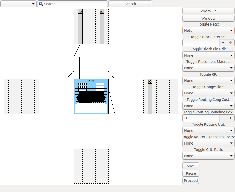
Fig. 3 blink.v circuit implementation on the EArch FPGA architecture as viewed in the VPR GUI
Automatically Running the VTR Flow
Running each stage of the flow manually is time consuming (and potentially error prone). For convenience, VTR provides a script (run_vtr_flow) which automates this process.
Lets make a new directory to work in named blink_run_flow:
> mkdir -p ~/vtr_work/quickstart/blink_run_flow
> cd ~/vtr_work/quickstart/blink_run_flow
Now lets run the script ($VTR_ROOT/vtr_flow/scripts/run_vtr_flow.pl) passing in:
The circuit verilog file (
$VTR_ROOT/doc/src/quickstart/blink.v)The FPGA architecture file (
$VTR_ROOT/vtr_flow/arch/timing/EArch.xml)
and also specifying the options:
-temp_dir .to run in the current directory (.on unix-like systems)--route_chan_width 100a fixed FPGA routing architecture channel width.
The resulting command is:
> $VTR_ROOT/vtr_flow/scripts/run_vtr_flow.pl \
    $VTR_ROOT/doc/src/quickstart/blink.v \
    $VTR_ROOT/vtr_flow/arch/timing/EArch.xml \
    -temp_dir . \
    --route_chan_width 100
Note
Options unrecognized by run_vtr_flow (like --route_chan_width) are passed on to VPR.
which should produce output similar to:
EArch/blink OK (took 0.26 seconds)
There are also multiple log files (including for ABC, ODIN and VPR), which by convention the script names with the .out suffix:
> ls *.out

0_blackboxing_latch.out  odin.out        report_clocks.abc.out  vanilla_restore_clocks.out
abc0.out                 report_clk.out  restore_latch0.out     vpr.out
With the main log files of interest including the ODIN log file (odin.out), log files produced by ABC (e.g. abc0.out), and the VPR log file (vpr.out).
Note
ABC may be invoked multiple times if a circuit has multiple clock domains, producing multiple log files (abc0.out, abc1.out, …)
You will also see there are several BLIF files produced:
> ls *.blif

0_blink.abc.blif   0_blink.raw.abc.blif  blink.odin.blif
0_blink.odin.blif  blink.abc.blif        blink.pre-vpr.blif
With the main files of interest being blink.odin.blif (netlist produced by ODIN), blink.abc.blif (final netlist produced by ABC after clock restoration), blink.pre-vpr.blif netlist used by VPR (usually identical to blink.abc.blif).
Like before, we can also see the implementation files generated by VPR:
> ls *.net *.place *.route

blink.net  blink.place  blink.route
which we can visualize with:
> $VTR_ROOT/vpr/vpr \
    $VTR_ROOT/vtr_flow/arch/timing/EArch.xml \
    blink --circuit_file blink.pre-vpr.blif \
    --route_chan_width 100 \
    --analysis --disp on
Next Steps
Now that you’ve finished the VTR quickstart, you’re ready to start experimenting and using VTR.
Here are some possible next steps for users wishing to use VTR:
Try modifying the Verilog file (e.g.
blink.v) or make your own circuit and try running it through the flow.Learn about FPGA architecture modelling (Tutorials, Reference), and try modifying a copy of
EArchto see how it changes the implementation ofblink.v.Read more about the VTR CAD Flow, and Task automation framework.
Find out more about using other benchmark sets, like how to run the Titan Benchmark Suite.
Discover how to generate FASM for bitstream creation.
Here are some possible next steps for developers wishing to modify and improve VTR:
Try the next steps listed for users above to learn how VTR is used.
Work through the new developer tutorial.
Read through the developer guide.
Look for open issues to which you can contribute.
Begin exploring the source code for the main tools in VTR (e.g. VPR in
$VTR_ROOT/vpr/src).